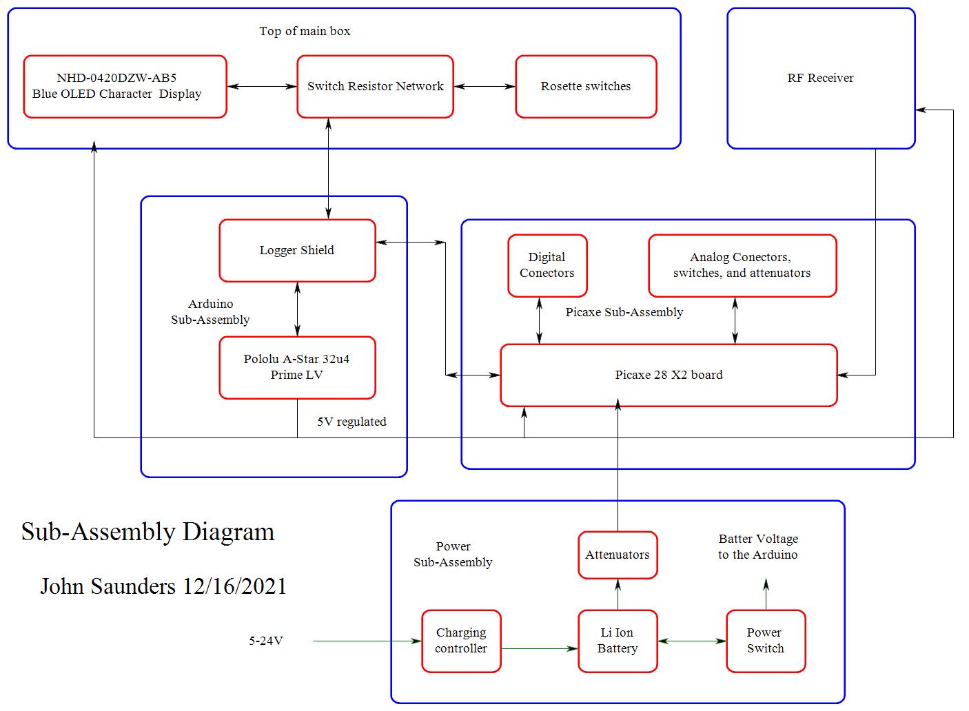
These are the logger circuit diagrams.
The circuit schematics are divided according to these five sub-assemblies, which are phsically separate and have minimized interconnections
|
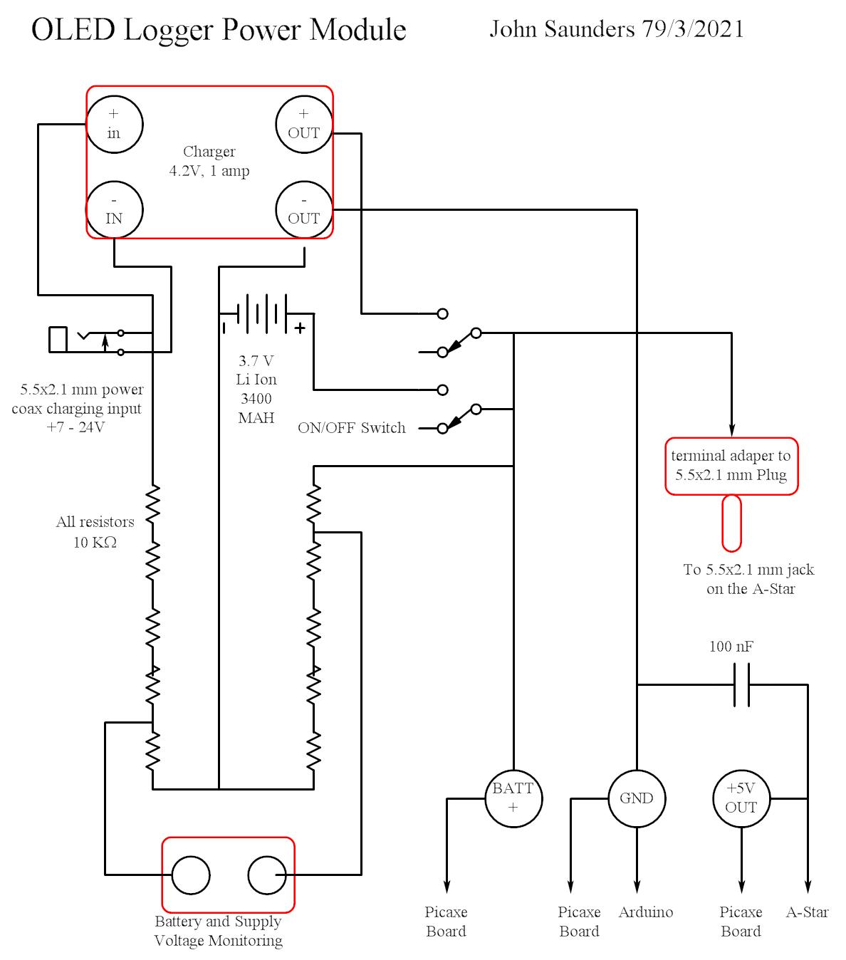
The Power Sub-Assembly switch is wired to isolate the battery when off.
|
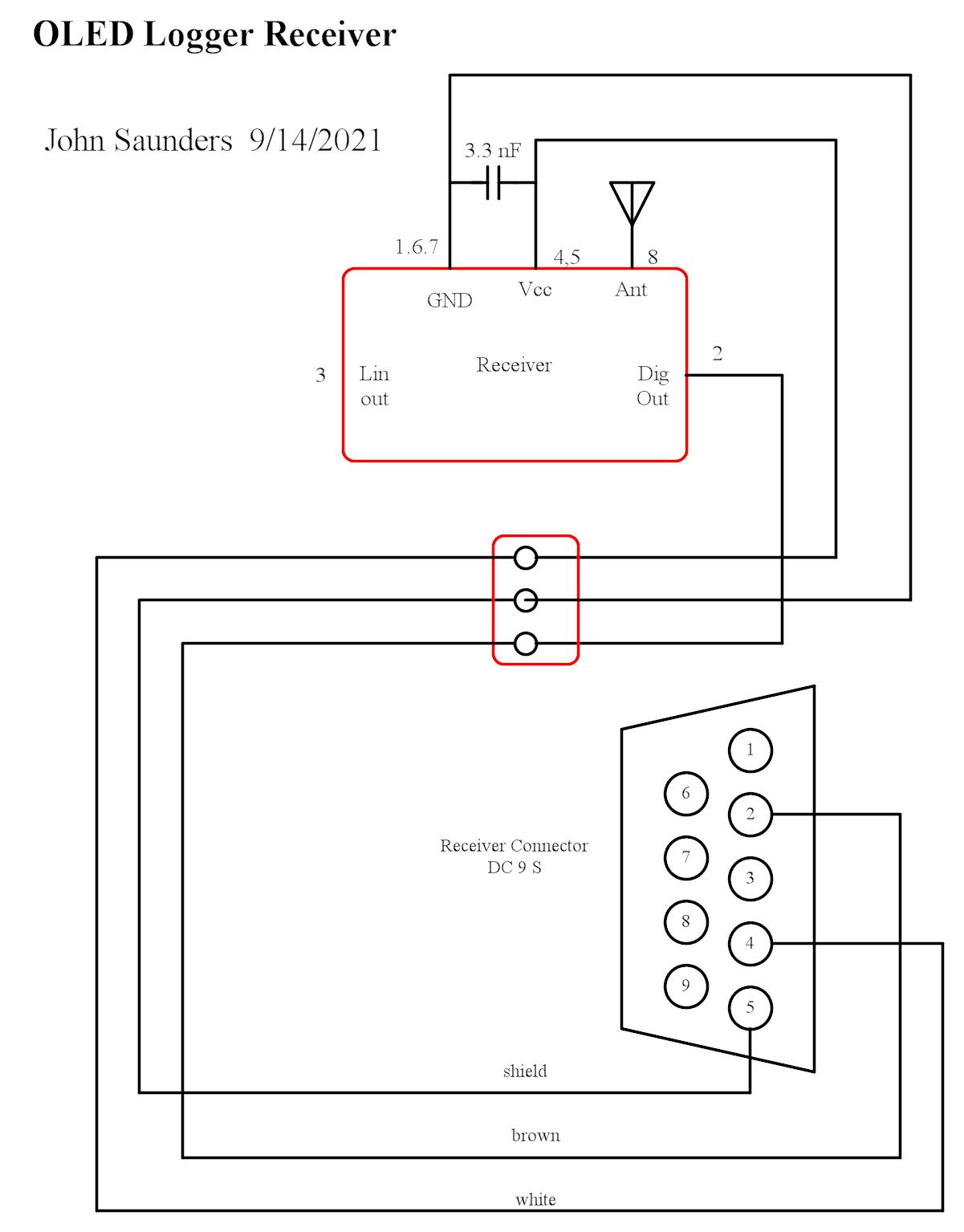
The RF Receiver is on the end of a short cable to keep it away from interference.
|
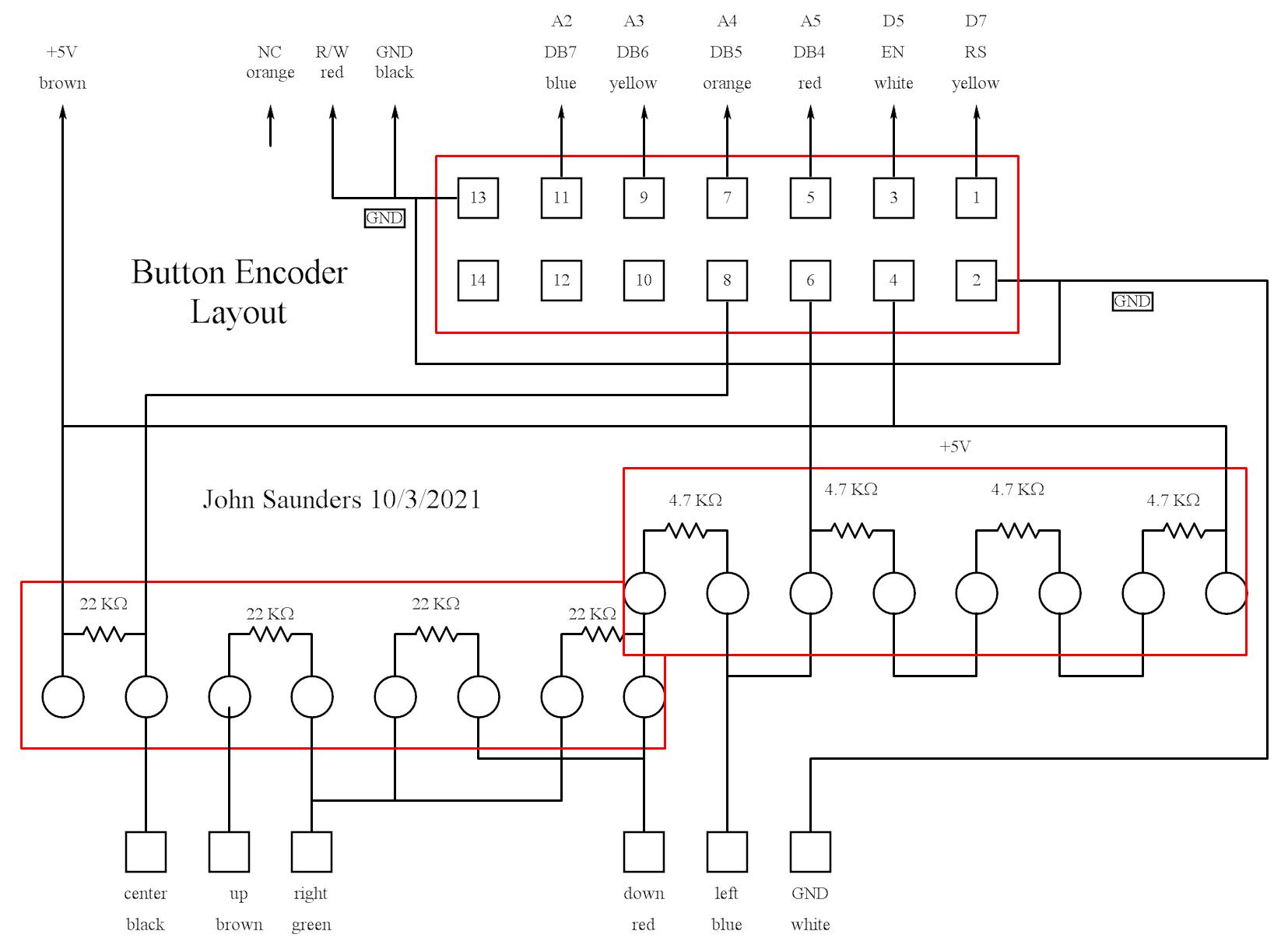
The top sub-Assembly has three units: The Display, the push-buttons, and the encoder.
|
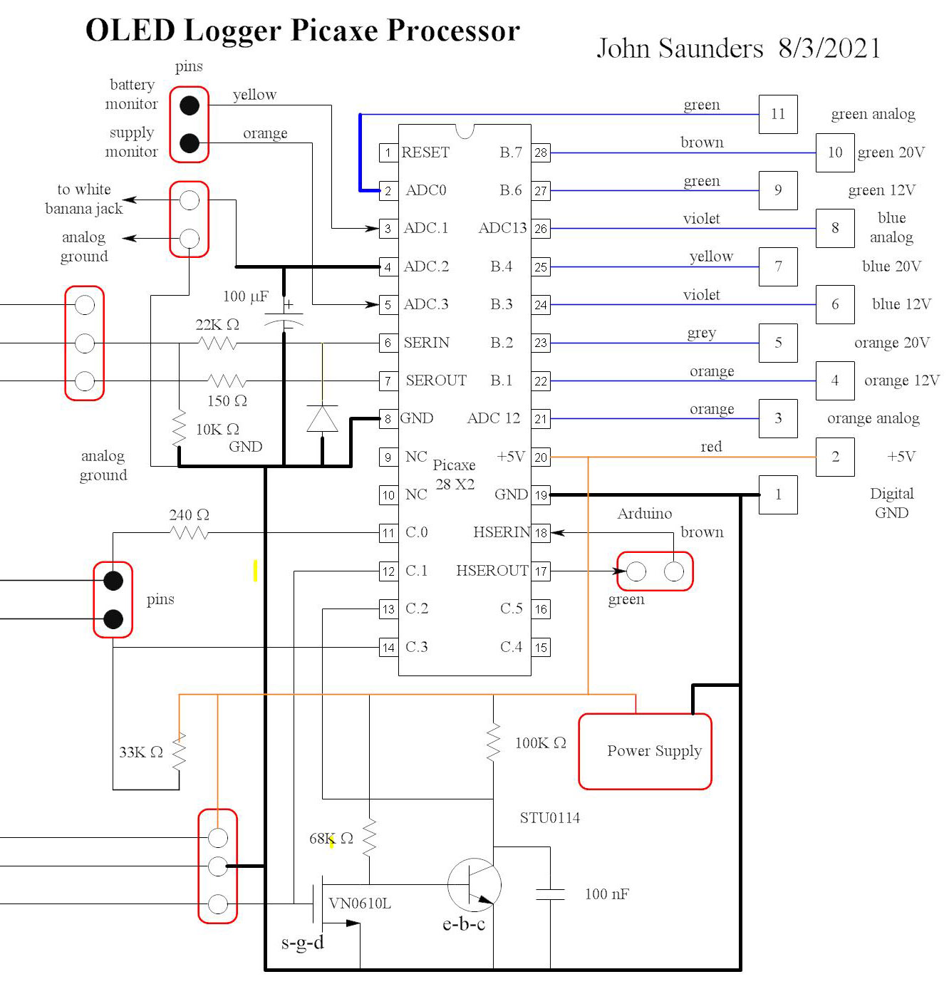
The Picaxe Processor Sub-assembly has many connections to the rear panel, but only 2 wires to the Logger Shield and two to the power sub-assembly monitor attenuators. The circuit at the bottom connects to the Receiver. It is an integrate-and-dump which has an output only for the 10 ms prepulse which precedes my messages. Noise and interference pulses rarely pass this circuit, which I have used in all my projects with receivers
|
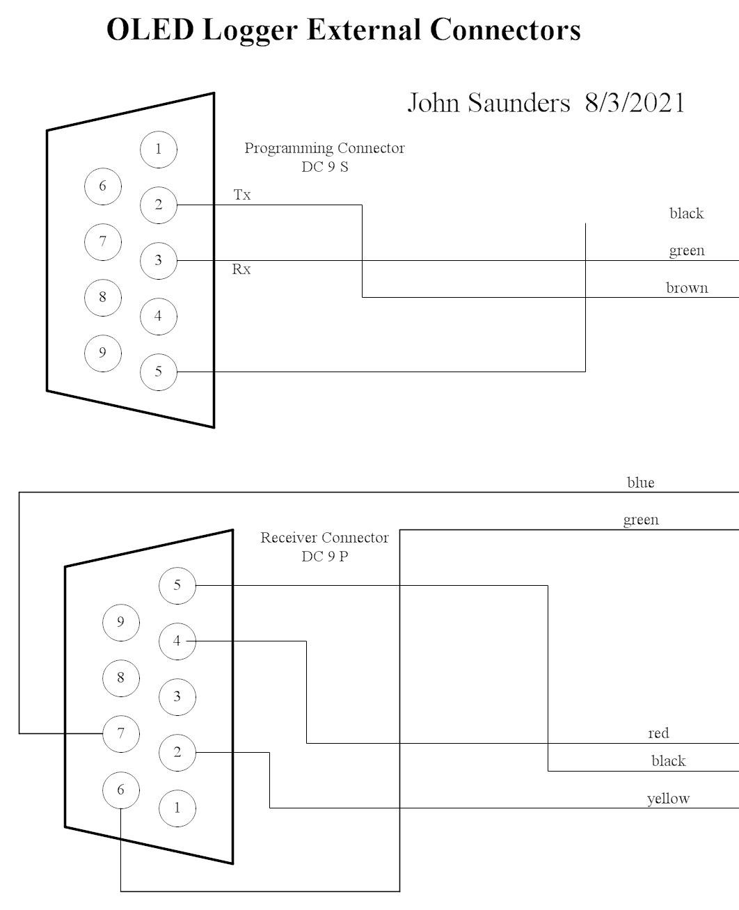
Rear Panel external connectors
|
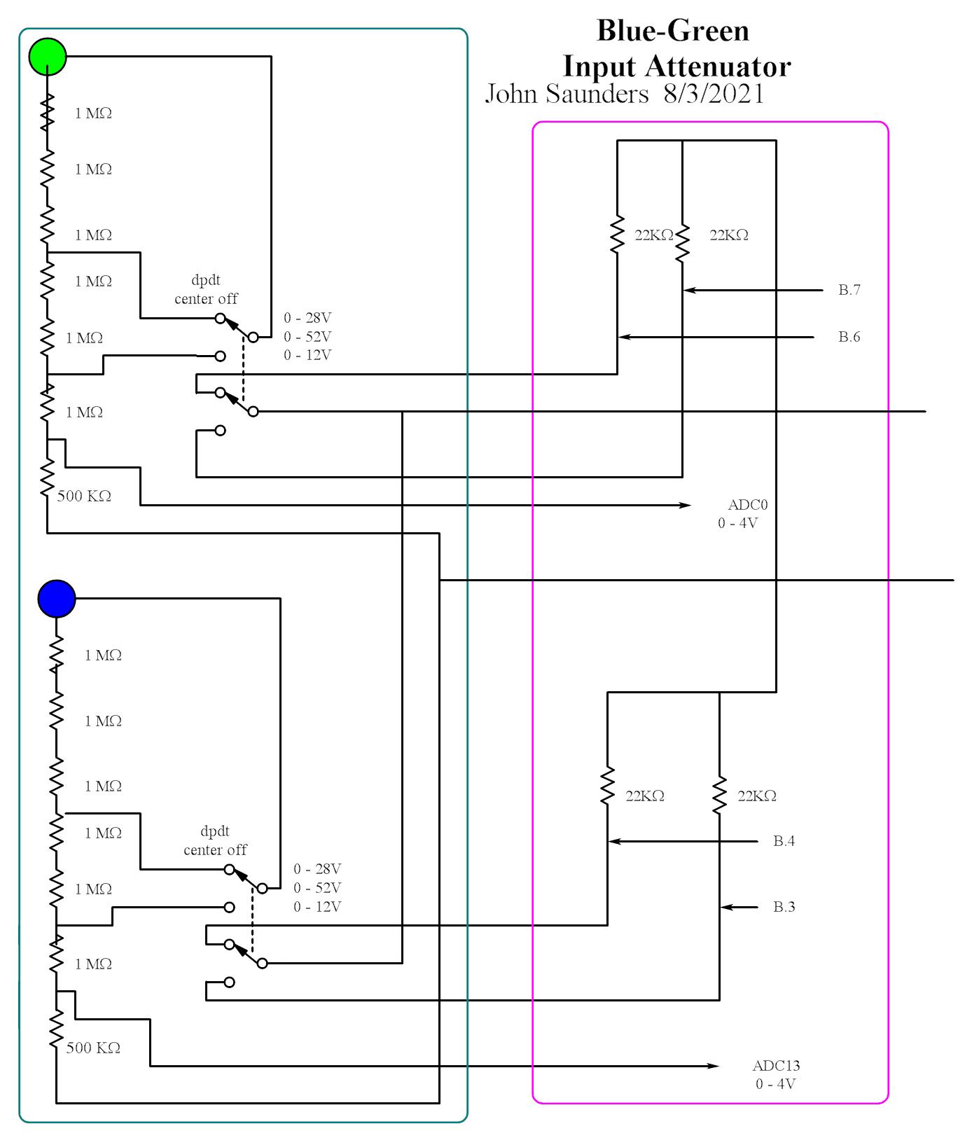
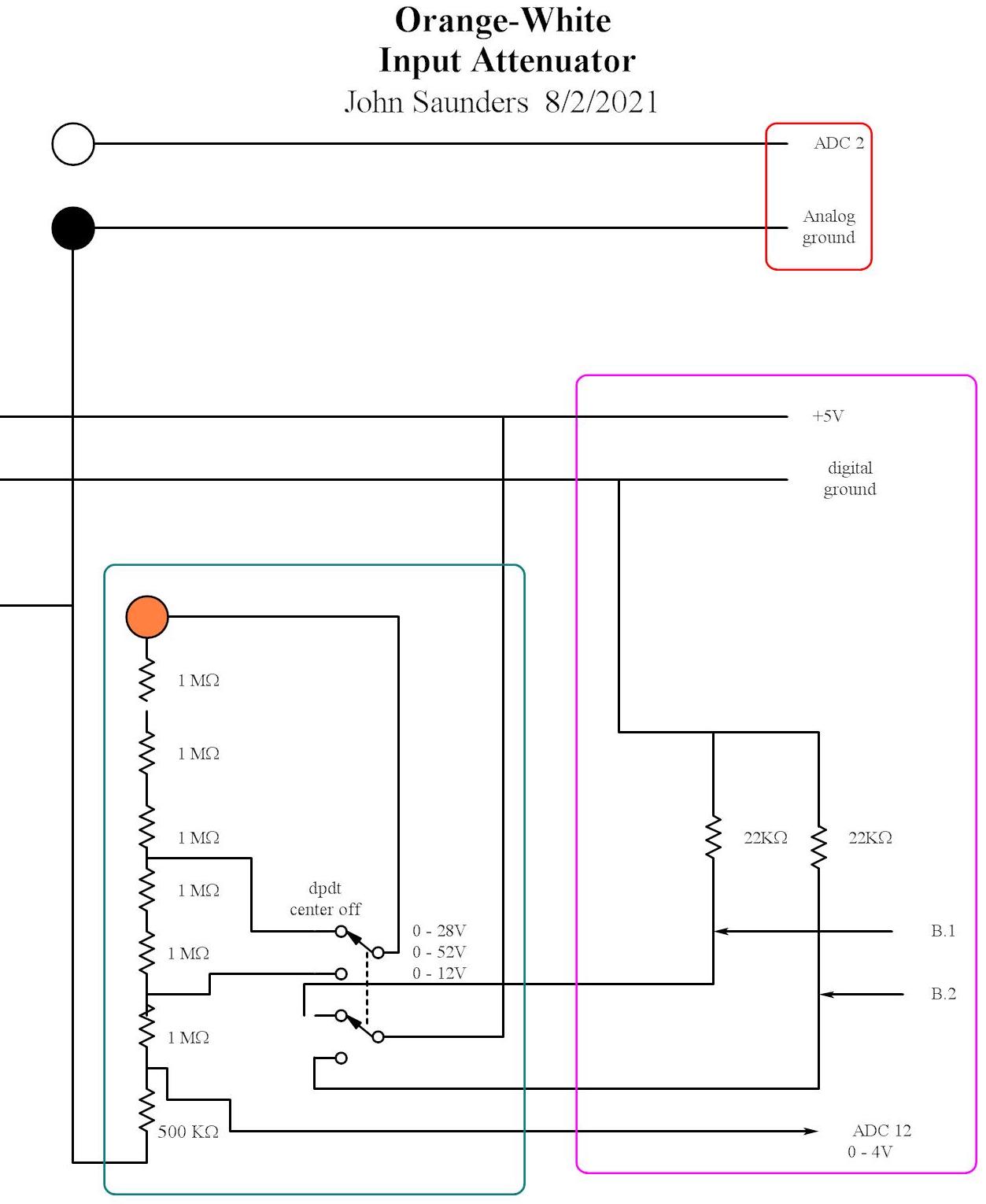
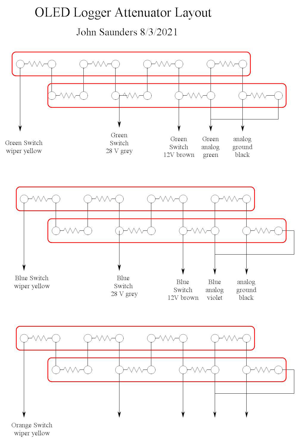
Rear Panel Analog Inputs The attenuators are constructed using SIP resistor packs, two per input. These have 4 equal individual resistors per pack. I use them freely since I bought hundreds cheaply in assortments.
|
|
This shows how wiring is minimized by paralleling two packs alongside each other. By paralleling the end two, ratios of 3,7 and 13 are achieved.
|
There is no circuit diagram for the Arduino sub-assembly because it is a standard configuration. |